PCB Production
Single sided PCB:
Single sided PCB is the simplest and most common type of PCB. It was the first device used for the interconnection and assembly of electronic components forming a coherent and functional operating system. The primary industry using these cards is the consumer electronics industry.
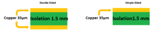
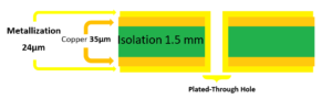
Double sided PCB:
The double-sided PCB is more complex than the single-sided PCB because it connects 2 faces of a circuit in 2 layers connected via PTH (Plated-Through Hole) which depends on the design
| Normes | Details | ||||||||||||||||||||||||||||||||||||||||||||||||||||||||||||||||||||||
| Currently, we accept the following PCB file formats:
In a zip or rar folder: _ Eagle file (.brd) _ Sprint layout file (lay / lay6) _ALtium file (.PcbDoc) _Proteus file (.lyt / psdsprj) _Adobe DXF file for Antennas. _Gerber files (See in details) |
In a zip or rar folder generate the following Gerber files with the RS-274-X format: GBL: Bottom Layer GBO: Bottom Overlay GBP: Bottom paste Mask GBS: Bottom Solder Mask GKO: Keep Out layer GTL: Top Layer GTO: Top Overlay GTS: TOP Solder Mask DRL / DRD : Drill file |
||||||||||||||||||||||||||||||||||||||||||||||||||||||||||||||||||||||
| FR4 Substat (1.6 mm)
|
|||||||||||||||||||||||||||||||||||||||||||||||||||||||||||||||||||||||
| PCB After Through-hole technology
|
|||||||||||||||||||||||||||||||||||||||||||||||||||||||||||||||||||||||
| Minimum track width 0.2 mm for PCB with high integration with an integrated SMD circuit |   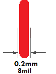 |
||||||||||||||||||||||||||||||||||||||||||||||||||||||||||||||||||||||
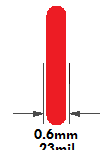
| Minimum track width 0.6 mm for ordinary circuit without ground plane | 
|
||||||||||||||||||||||||||||||||||||||||||||||||||||||||||||||||||||||
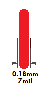
| Track width 0.18mm for a maximum length of 10mm
Use this width only in short distances |
 |
||||||||||||||||||||||||||||||||||||||||||||||||||||||||||||||||||||||
| Distance minimale entre deux pistes : 0.2 mm | 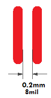 |
||||||||||||||||||||||||||||||||||||||||||||||||||||||||||||||||||||||
| Minimum distance between track and via: 0.25 mm | 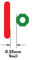 |
||||||||||||||||||||||||||||||||||||||||||||||||||||||||||||||||||||||
| Minimum distance between track and pad: 0.3 mm | 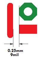 |
||||||||||||||||||||||||||||||||||||||||||||||||||||||||||||||||||||||
| Minimum distance between track and frame: 0.3 mm | 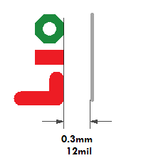 |
||||||||||||||||||||||||||||||||||||||||||||||||||||||||||||||||||||||
| Insulation between the circuit and the ground plane 0.3 mm | 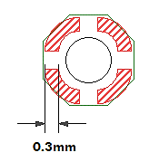 |
||||||||||||||||||||||||||||||||||||||||||||||||||||||||||||||||||||||
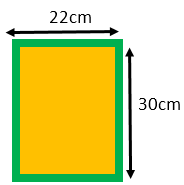
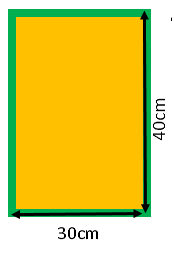
| Maximum and minimum size of PCB boards | PCB single sided : 30×40 cm²
PCB double sided : 22×30 cm²
Minimum dimensions for single / double sided PCB: 2x2cm²
|
||||||||||||||||||||||||||||||||||||||||||||||||||||||||||||||||||||||
| Minimum thickness for a patch between 0.4 and 0.5 mm | 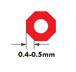 |
||||||||||||||||||||||||||||||||||||||||||||||||||||||||||||||||||||||
| Minimum distance between two via or two fixing holes 0.3mm | 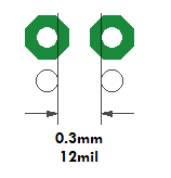 |
||||||||||||||||||||||||||||||||||||||||||||||||||||||||||||||||||||||
| Never put two via or two fixing holes interposed | 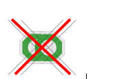 |
||||||||||||||||||||||||||||||||||||||||||||||||||||||||||||||||||||||
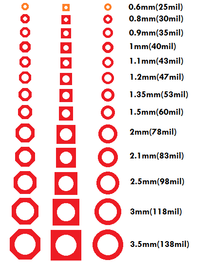
| The minimum dimension for a via: 0.6 mm
The maximum dimension for hole is 3.5 mm |
 |
||||||||||||||||||||||||||||||||||||||||||||||||||||||||||||||||||||||
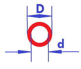
| D : patch diameter
d : hole diameter
|
|
||||||||||||||||||||||||||||||||||||||||||||||||||||||||||||||||||||||